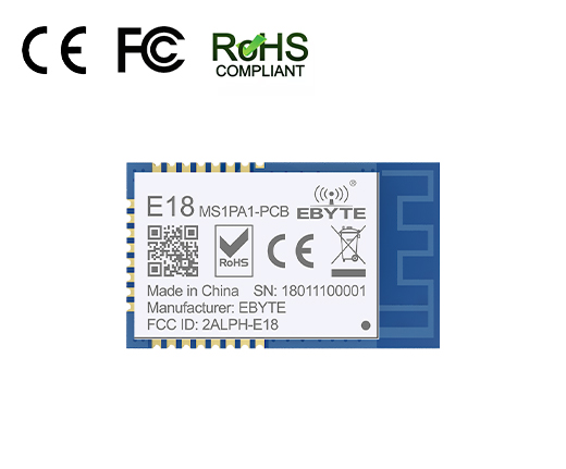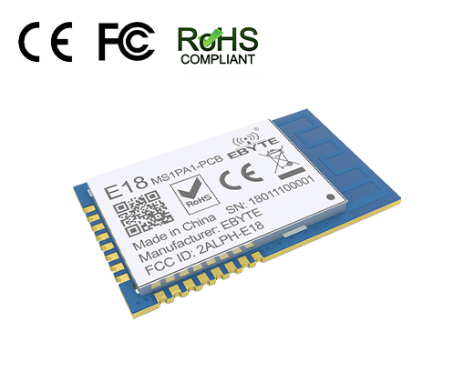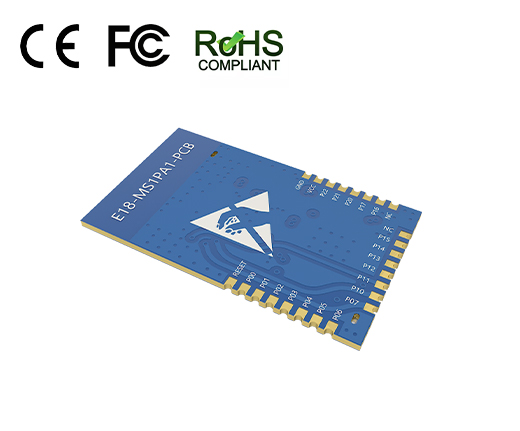

E18-MS1PA1-PCB CC2530 2.4GHz Zigbee cdebyte PA Wireless RFID Transceiver Module PA PCB Antenna I / O Port IoT Data Transceiver
[IC]:CC2530
[Frequency]:2.4~2.48GHz
[Power]:20dBm
[Distance]:0.8km
[Interface]:IO
[Weight]:1.8±0.1g
[Introduction]:E18-MS1PA1-PCB is based on original imported RF chip CC2530 form TI in America. The IC chip is integrated with 8051 microcontroller and wireless transceiver, which is applicable to Zigbee design and 2.4GHz IEEE 802.15.4 protocol and equipped with power amplifier chip CC2592, the transmitting range is much longer than before.
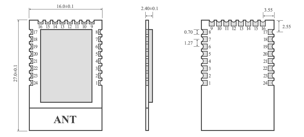
| Pin number | CC2530 Pin name | Module Pin name | Input/Output | Pin usage |
| l | GND | GND | Ground wire,connected to the power reference ground | |
| 2 | vcc | voc | Power supply,must be between 1.8 ~3.6v | |
| 3 | P2.2 | GPIO | 1/o | DC-download program or Debug clock interface |
| 4 | P2.1 | GPIO | I/o | DD-download program or Debug data interface |
| 5 | P2.0 | GPIO | I/o | wc |
| 6 | p1.7 | NWK_KEY | lused for manua1 join,exit,and quick match keys. Not networked: Short press to join the network or create a network operation; Networked: Short press for quick match; Long press means to leave the current network; Note: Low level is valid,100ms≤short press名 3000ms,5000≤long press. | |
| 7 | P1.6 | GPIO | 1/o | N/c |
| 8 | NC | NC | N/c | |
| g | NC | NC | w/c | |
| 10 | Pl.5 | UARTO_Tx | I | Serial port TX pin |
| 11 | P1.4 | UARTO_RX | o | Serial port RX pin |
| 12 | P1.3 | RUN_LED | o | It is used to indicate the network access status of the module. Fast flashing 256 times (10Hz frequcncy) indicates that it is joining the network or creating a network,and slow flashing 12 times(2lE frequency) indicates that the module has joined the network or successfully created the network; Low level lights up: |
| 13 | P1.2 | NWK_LED | It is used to indicate the one key pairing status of the module,provided that two modules need to join the same coordinator,and then one key pairing can be performed. In the transparent mode,mutual transparent transmission can be performed. Low level lighting: | |
| 14 | P1.1 | I/O | The PA transmit control pin has been connected inside the module; There is no PA inside the E18-MS1-PCB/E18-MS1-IPX; | |
| 15 | P1.0 | GPIo | I/O | The PA receiving control pin has been connected inside the module; There is no PA inside the E18-MS1-PCB/E18-MS1-IPX; |
| 16 | PO.7 | HGM | O | HCM pin of PA; E18-MS1-PCB/E18-MS1-IPX has no PA inside,so this pin is used as GP10 port; |
| 17 | P0.6 | GPIO | I/O | N/C |
| 18 | P0.5 | cPIO | I/O | N/C |
| 19 | PO.4 | cPIO | I/O | N/C |
| 20 | P0.3 | CPIo | I/O | N/C |
| 21 | PO.2 | cPIo | I/O | N/C |
| 22 | PO.1 | cPI0 | I/O | N/C |
| 23 | Po.0 | GPI0 | I/O | N/C |
| 24 | RESET | RESET | I | Reset port |


